_______________General Description
The MAX7219/MAX7221 are compact, serial input/out-put common-cathode display drivers that interface microprocessors (µPs) to 7-segment numeric LED dis-plays of up to 8 digits, bar-graph disdis-plays, or 64 indi-vidual LEDs. Included on-chip are a BCD code-B decoder, multiplex scan circuitry, segment and digit drivers, and an 8x8 static RAM that stores each digit. Only one external resistor is required to set the seg-ment current for all LEDs. The MAX7221 is compatible with SPI™, QSPI™, and Microwire™, and has slew-rate-limited segment drivers to reduce EMI.A convenient 3-wire serial interface connects to all common µPs. Individual digits may be addressed and updated without rewriting the entire display. The MAX7219/MAX7221 also allow the user to select code-B decoding or no-decode for each digit.
The devices include a 150µA low-power shutdown mode, analog and digital brightness control, a scan-limit register that allows the user to display from 1 to 8 digits, and a test mode that forces all LEDs on.
________________________Applications
Bar-Graph Displays7-Segment Displays Industrial Controllers Panel Meters LED Matrix Displays
____________________________Features
♦ 10MHz Serial Interface♦ Individual LED Segment Control ♦ Decode/No-Decode Digit Selection
♦ 150µA Low-Power Shutdown (Data Retained)
♦ Digital and Analog Brightness Control ♦ Display Blanked on Power-Up
♦ Drive Common-Cathode LED Display
♦ Slew-Rate Limited Segment Drivers for Lower EMI (MAX7221)
♦ SPI, QSPI, Microwire Serial Interface (MAX7221) ♦ 24-Pin DIP and SO Packages
MAX7219/MAX7221
________________________________________________________________Maxim Integrated Products 1
( ) MAX7221 ONLY 8-DIGIT µP DISPLAY
DIG 0–DIG 7 MOSI I/O SCK 18 1 12 13 9 4 DIN µP ISET 9.53k 8 DIGITS 8 SEGMENTS +5V 19 SEG A–G, SEG DP CLK LOAD (CS) GND V+ GND MAX7219 MAX7221
________Typical Application Circuit
__________________Pin Configuration
24 23 22 21 20 19 18 17 1 2 3 4 5 6 7 8 DOUT SEG D SEG DP SEG E GND DIG 4 DIG 0 DIN TOP VIEW SEG C V+ ISET SEG G DIG 7 DIG 3 DIG 2 DIG 6 16 15 14 13 9 10 11 12 SEG B SEG F SEG A CLK ( ) MAX7221 ONLY LOAD (CS) DIG 1 DIG 5 GND DIP/SO MAX7219 MAX7221 PART MAX7219CNG MAX7219CWG MAX7219C/D 0°C to +70°C 0°C to +70°C 0°C to +70°CTEMP. RANGE PIN-PACKAGE
24 Narrow Plastic DIP 24 Wide SO
Dice*
______________Ordering Information
Ordering Information continued at end of data sheet.
*Dice are specified at TA = +25°C.
MAX7219ENG MAX7219EWG
MAX7219ERG -40°C to +85°C -40°C to +85°C
-40°C to +85°C 24 Narrow Plastic DIP 24 Wide SO
24 Narrow CERDIP
SPI and QSPI are trademarks of Motorola Inc. Microwire is a trademark of National Semiconductor Corp.
MAX7219/MAX7221
ABSOLUTE MAXIMUM RATINGS
ELECTRICAL CHARACTERISTICS
(V+ = 5V ±10%, RSET = 9.53kΩ±1%, TA= TMINto TMAX, unless otherwise noted.)
Stresses beyond those listed under “Absolute Maximum Ratings” may cause permanent damage to the device. These are stress ratings only, and functional operation of the device at these or any other conditions beyond those indicated in the operational sections of the specifications is not implied. Exposure to absolute maximum rating conditions for extended periods may affect device reliability.
Voltage (with respect to GND)
V+ ...-0.3V to 6V DIN, CLK, LOAD, CS ...-0.3V to 6V
All Other Pins...-0.3V to (V+ + 0.3V) Current
DIG0–DIG7 Sink Current...500mA SEGA–G, DP Source Current...100mA Continuous Power Dissipation (TA= +85°C)
Narrow Plastic DIP ...0.87W Wide SO ...0.76W Narrow CERDIP...1.1W
Operating Temperature Ranges
MAX7219C_G/MAX7221C_G ...0°C to +70°C MAX7219E_G/MAX7221E_G ...-40°C to +85°C Storage Temperature Range ...-65°C to +160°C Lead Temperature (soldering, 10sec) ...+300°C
RSET= open circuit
All digital inputs at V+ or GND, TA= +25°C
Digit off, VDIGIT= V+
TA= +25°C, V+ = 5V, VOUT= (V+ - 1V)
All segments and decimal point on, ISEG_= -40mA 8 digits scanned V+ = 5V, VOUT= 0.65V TA= +25°C, V+ = 5V, VOUT= (V+ - 1V) CONDITIONS 8 Operating Supply Current
µA 150 I+ V 4.0 5.5 V+ Operating Supply Voltage
Shutdown Supply Current
µA -10
IDIGIT
Digit Drive Leakage (MAX7221 only)
% 3.0
∆ISEG
Segment Drive Current Matching
mA/µs 10 20 50
∆ISEG/∆t
Segment Current Slew Rate (MAX7221 only) mA 330 I+ Hz 500 800 1300 fOSC
Display Scan Rate
mA 320
IDIGIT
Digit Drive Sink Current
mA -30 -40 -45
ISEG
Segment Drive Source Current
UNITS
MIN TYP MAX
SYMBOL PARAMETER
Segment off, VSEG= 0V 1 µA
ISEG
Segment Drive Leakage (MAX7221 only)
Digit off, VDIGIT= (V+ - 0.3V) -2 mA IDIGIT
Digit Drive Source Current (MAX7219 only)
Segment off, VSEG= 0.3V 5 mA
ISEG
Segment Drive Sink Current (MAX7219 only)
MAX7219/MAX7221
ELECTRICAL CHARACTERISTICS (continued)
(V+ = 5V ±10%, RSET =9.53kΩ±1%, TA= TMINto TMAX, unless otherwise noted.)
VIN= 0V or V+
DOUT, ISINK= 1.6mA
DOUT, ISOURCE= -1mA
CONDITIONS
µA
-1 1
IIH, IIL
Input Current DIN, CLK, LOAD, CS
V 0.4 VOL
Output Low Voltage
V 3.5
VIH
Logic High Input Voltage
V 0.8 VIL
Logic Low Input Voltage
V V+ - 1
VOH
Output High Voltage
UNITS
MIN TYP MAX
SYMBOL PARAMETER DIN, CLK, LOAD, CS 1 V ∆VI Hysteresis Voltage ns 25 tCSS
CS Fall to SCLK Rise Setup Time (MAX7221 only) ns 100 tCP CLK Clock Period ns 50 tCH
CLK Pulse Width High
ns 50
tCL
CLK Pulse Width Low
CLOAD= 50pF
ns 25
tDS
DIN Setup Time
ns 50
tCSW
Minimum CS or LOAD Pulse High
ns 0
tDH
DIN Hold Time
ns 25
tDO
Output Data Propagation Delay
ns 50
tLDCK
Load-Rising Edge to Next Clock Rising Edge (MAX7219 only)
ns 0
tCSH
CLK Rise to CS or LOAD Rise Hold Time ms 2.25 tDSPD Data-to-Segment Delay LOGIC INPUTS TIMING CHARACTERISTICS
MAX7219/MAX7221
__________________________________________Typical Operating Characteristics
(V+ = +5V, TA = +25°C, unless otherwise noted.)
730 750 740 770 760 790 780 800 820 810 830 4.0 4.4 4.8 5.2 5.6 6.0 SCAN FREQUENCY vs. POSITIVE SUPPLY VOLTAGE
MAX7219/21 01
POSITIVE SUPPLY VOLTAGE (V)
SCAN FREQUENCY (Hz) 0 20 10 40 30 60 50 70 0 1 2 3 4 5
SEGMENT DRIVER OUTPUT CURRENT vs. OUTPUT VOLTAGE
MAX7219/21 02
OUTPUT VOLTAGE (V)
OUTPUT CURRENT (mA)
RSET = 10kΩ
RSET = 20kΩ
RSET = 40kΩ
MAX7219 SEGMENT OUTPUT CURRENT
MAX7219/21 03 5µs/div 10mA/div 0 MAXIMUM INTENSITY = 31/32 MAX7221 SEGMENT OUTPUT CURRENT
MAX7219/21 04
5µs/div 10mA/div
0
MAX7219/MAX7221
______________________________________________________________Pin Description
_________________________________________________________Functional Diagram
NAME FUNCTION
1 DIN Serial-Data Input. Data is loaded into the internal 16-bit shift register on CLK’s rising edge. 2, 3, 5–8,
10, 11 DIG 0–DIG 7
Eight-Digit Drive Lines that sink current from the display common cathode. The MAX7219 pulls the digit outputs to V+ when turned off. The MAX7221’s digit drivers are high-impedance when turned off.
PIN
4, 9 GND Ground (both GND pins must be connected)
12
LOAD (MAX7219)
18 ISET Connect to VDDthrough a resistor (RSET) to set the peak segment current (Refer to Selecting RSETResistor section).
14–17, 20–23 SEG A–SEG G, DP 13 CLK CS (MAX7221)
24 DOUT Serial-Data Output. The data into DIN is valid at DOUT 16.5 clock cycles later. This pin is used to daisy-chain several MAX7219/MAX7221’s and is never high-impedance.
19 V+ Positive Supply Voltage. Connect to +5V.
( ) MAX7221 ONLY V+ 8 8 8 8 4 RSET LOAD (CS) DIN DOUT CLK (MSB) (LSB) D0
SEG A–SEG G, DP DIG 0–DIG 7
SHUTDOWN REGISTER MODE REGISTER INTENSITY REGISTER SCAN-LIMIT REGISTER DISPLAY-TEST REGISTER INTENSITY PULSE-WIDTH MODULATOR MULTIPLEX SCAN CIRCUITRY ADDRESS REGISTER DECODER 8x8 DUAL-PORT SRAM 8 D1 D2 D3 D4 D5 D6 D7 D8 D9 D10 D11 D12 DIGIT DRIVERS D13 D14 D15 CODE B ROM WITH BYPASS SEGMENT CURRENT REFERENCE SEGMENT DRIVERS
Load-Data Input. The last 16 bits of serial data are latched on LOAD’s rising edge.
Chip-Select Input. Serial data is loaded into the shift register while CS is low. The last 16 bits of serial data are latched on CS’s rising edge.
Serial-Clock Input. 10MHz maximum rate. On CLK’s rising edge, data is shifted into the inter-nal shift register. On CLK’s falling edge, data is clocked out of DOUT. On the MAX7221, the CLK input is active only while CS is low.
Seven Segment Drives and Decimal Point Drive that source current to the display. On the MAX7219, when a segment driver is turned off it is pulled to GND. The MAX7221 segment dri-vers are high-impedance when turned off.
MSB
MAX7219/MAX7221
_______________Detailed Description
MAX7219/MAX7221 Differences
The MAX7219 and MAX7221 are identical except for two parameters: the MAX7221 segment drivers are slew-rate limited to reduce electromagnetic interfer-ence (EMI), and its serial interface is fully SPI compati-ble.
Serial-Addressing Modes
For the MAX7219, serial data at DIN, sent in 16-bit packets, is shifted into the internal 16-bit shift register with each rising edge of CLK regardless of the state of LOAD. For the MAX7221, CS must be low to clock data in or out. The data is then latched into either the digit or control registers on the rising edge of LOAD/CS. LOAD/CS must go high concurrently with or after the 16th rising clock edge, but before the next rising clock edge or data will be lost. Data at DIN is propagated through the shift register and appears at DOUT 16.5 clock cycles later. Data is clocked out on the falling edge of CLK. Data bits are labeled D0–D15 (Table 1). D8–D11 contain the register address. D0–D7 contain the data, and D12–D15 are “don’t care” bits. The first received is D15, the most significant bit (MSB).
Digit and Control Registers
Table 2 lists the 14 addressable digit and control regis-ters. The digit registers are realized with an on-chip, 8x8 dual-port SRAM. They are addressed directly so that individual digits can be updated and retain data as long as V+ typically exceeds 2V. The control registers consist of decode mode, display intensity, scan limit (number of scanned digits), shutdown, and display test (all LEDs on).
Shutdown Mode
When the MAX7219 is in shutdown mode, the scan oscil-lator is halted, all segment current sources are pulled to ground, and all digit drivers are pulled to V+, thereby blanking the display. The MAX7221 is identical, except the drivers are high-impedance. Data in the digit and control registers remains unaltered. Shutdown can be used to save power or as an alarm to flash the display by successively entering and leaving shutdown mode. For minimum supply current in shutdown mode, logic inputs should be at ground or V+ (CMOS-logic levels).
Typically, it takes less than 250µs for the MAX7219/ MAX7221 to leave shutdown mode. The display driver can be programmed while in shutdown mode, and shutdown mode can be overridden by the display-test function. CLK DIN D15 DOUT D14 D1 D0 tCSS tCL tCH tCP tDO tLDCK tCSW tCSH tDS tDH CS OR LOAD
Figure 1. Timing Diagram
Table 1. Serial-Data Format (16 Bits)
D14 D15 X D12 D13 X X D10 D11 D9 D8 ADDRESS D6 D7 D5 D4 X D2 D3 D1 D0 MSB DATA LSB
Initial Power-Up
On initial power-up, all control registers are reset, the display is blanked, and the MAX7219/MAX7221 enter shutdown mode. Program the display driver prior to display use. Otherwise, it will initially be set to scan one digit, it will not decode data in the data registers, and the intensity register will be set to its minimum value.
Decode-Mode Register
The decode-mode register sets BCD code B (0-9, E, H, L, P, and -) or no-decode operation for each digit. Each bit in the register corresponds to one digit. A logic high selects code B decoding while logic low bypasses the decoder. Examples of the decode mode control-regis-ter format are shown in Table 4.
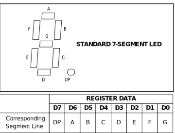
When the code B decode mode is used, the decoder looks only at the lower nibble of the data in the digit registers (D3–D0), disregarding bits D4–D6. D7, which sets the decimal point (SEG DP), is independent of the decoder and is positive logic (D7 = 1 turns the decimal point on). Table 5 lists the code B font.
When no-decode is selected, data bits D7–D0 corre-spond to the segment lines of the MAX7219/MAX7221. Table 6 shows the one-to-one pairing of each data bit to the appropriate segment line.
MAX7219/MAX7221
Table 2. Register Address Map
Table 3. Shutdown Register Format (Address (Hex) = XC)
Table 4. Decode-Mode Register Examples (Address (Hex) = X9)
No-Op X 0 0 0 0 0 ADDRESS 0 1 X0 X1 Digit 1 X 0 0 0 1 1 0 1 X2 0 X3 0 Digit 2 X Digit 3 X 0 1 1 0 Digit 0 X 0 0 1 X4 X5 Digit 5 X 0 1 1 1 1 0 1 X6 0 X7 0 Digit 6 X Digit 4 X Digit 7 X 1 0 0 0 0 0 1 X8 X9 1 Decode Mode X Intensity X 1 0 0 1 1 0 1 XA XB Shutdown X 1 1 1 0 1 0 1 XC 1 XF 1 Display Test X Scan Limit X D15– D12 D11 D10 REGISTER D9 D8 HEX CODE X Shutdown Mode XC X X X X X X X X X 0 X 1 X X X REGISTER DATA MODE Normal Operation XC 0
No decode for digits 7–0 0 0 1 D7 DECODE MODE 0 0 00 0 1 D6 D5 0 1 D4 D3 0 1 Code B decode for digits 7–0
Code B decode for digit 0 No decode for digits 7–1
0 0 0 1 D2 HEX CODE 0 REGISTER DATA 0 FF 1 1 D1 D0 0 1 0 1 0 0 0 01 0
Code B decode for digits 3–0
No decode for digits 7–4 1 1 1 1 0F
ADDRESS CODE
MAX7219/MAX7221
Intensity Control and Interdigit Blanking
The MAX7219/MAX7221 allow display brightness to be controlled with an external resistor (RSET) connected
between V+ and ISET. The peak current sourced from the segment drivers is nominally 100 times the current entering ISET. This resistor can either be fixed or vari-able to allow brightness adjustment from the front panel. Its minimum value should be 9.53Ω, which typi-cally sets the segment current at 40mA. Display bright-ness can also be controlled digitally by using the intensity register.
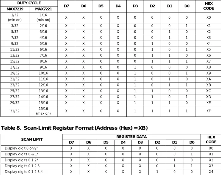
Digital control of display brightness is provided by an internal pulse-width modulator, which is controlled by the lower nibble of the intensity register. The modulator scales the average segment current in 16 steps from a maximum of 31/32 down to 1/32 of the peak current set by RSET (15/16 to 1/16 on MAX7221). Table 7 lists the
intensity register format. The minimum interdigit blank-ing time is set to 1/32 of a cycle.
Table 5. Code B Font
Table 6. No-Decode Mode Data Bits and
Corresponding Segment Lines
0 X 0 0 0 0 1 1 1 1 1 1 D7* REGISTER DATA 0 7-SEGMENT CHARACTER D6–D4 D3 D2 D1 D0 DP* A B C D E F G 1 X 0 0 0 1 0 1 ON SEGMENTS = 1 0 1 0 0 0 2 X 0 0 1 0 1 1 0 1 1 0 1 3 X 0 0 1 1 1 1 1 1 0 0 1 4 X 0 1 0 0 0 1 1 0 0 1 1 5 X 0 1 0 1 1 0 1 1 0 1 1 6 X 0 1 1 0 1 0 1 1 1 1 1 7 X 0 1 1 1 1 1 1 0 0 0 0 8 X 1 0 0 0 1 1 1 1 1 1 1 9 X 1 0 0 1 1 1 1 1 0 1 1 — X 1 0 1 0 0 0 0 0 0 0 1 E X 1 0 1 1 1 0 0 1 1 1 1 H X 1 1 0 0 0 1 1 0 1 1 1 L X 1 1 0 1 0 0 0 1 1 1 0 P X 1 1 1 0 1 1 0 0 1 1 1 blank X 1 1 1 1 0 0 0 0 0 0 0
*The decimal point is set by bit D7 = 1
F E A G D C B
STANDARD 7-SEGMENT LED
DP A Corresponding Segment Line D6 DP C D4 B D5 E D2 D G REGISTER DATA D0 F D1 D3 D7
Scan-Limit Register
The scan-limit register sets how many digits are dis-played, from 1 to 8. They are displayed in a multiplexed manner with a typical display scan rate of 800Hz with 8 digits displayed. If fewer digits are displayed, the scan rate is 8fOSC/N, where N is the number of digits
scanned. Since the number of scanned digits affects the display brightness, the scan-limit register should not be used to blank portions of the display (such as leading zero suppression). Table 8 lists the scan-limit register format.
MAX7219/MAX7221
Table 7. Intensity Register Format (Address (Hex) = XA)
DUTY CYCLE MAX7221 MAX7219 D7 D6 D5 D4 D3 D2 D1 D0 HEX CODE 1/16 (min on) 1/32 (min on) X X X X 0 0 0 0 X0 2/16 3/32 X X X X 0 0 0 1 X1 3/16 5/32 X X X X 0 0 1 0 X2 4/16 7/32 X X X X 0 0 1 1 X3 5/16 9/32 X X X X 0 1 0 0 X4 6/16 11/32 X X X X 0 1 0 1 X5 7/16 13/32 X X X X 0 1 1 0 X6 X 8/16 15/32 X X X X 1 0 1 1 X7 9/16 17/32 X X X X 0 1 0 0 X8 10/16 19/32 X X X X 0 1 0 1 X9 11/16 21/32 X X X X 0 1 1 0 XA 12/16 23/32 X X X X 0 1 1 1 XB 13/16 25/32 X X X X 1 1 0 0 XC 14/16 27/32 X X X X 1 1 0 1 XD 15/16 29/32 X X X X 1 1 1 0 XE 15/16 (max on) 31/32 X X X 1 1 1 1 XFTable 8. Scan-Limit Register Format (Address (Hex) = XB)
X X Display digit 0 only*
Display digits 0 & 1*
X X X D7 SCAN LIMIT X1 X X0 X X X 0 D6 D5 0 1 D4 D3 X X Display digits 0 1 2* Display digits 0 1 2 3 X X X X 0 X3 X D2 HEX CODE X2 0 REGISTER DATA 0 X X X D1 D0 0 1 1 X 0 1 0 X X Display digits 0 1 2 3 4 Display digits 0 1 2 3 4 5 X X X X5 X X4 X X X 1 0 1 X X Display digits 0 1 2 3 4 5 6 Display digits 0 1 2 3 4 5 6 7 X X X X 1 X7 X X6 0 0 X X X 1 1 1 X 1 1 0
MAX7219/MAX7221
If the scan-limit register is set for three digits or less, individual digit drivers will dissipate excessive amounts of power. Consequently, the value of the RSETresistor
must be adjusted according to the number of digits dis-played, to limit individual digit driver power dissipation. Table 9 lists the number of digits displayed and the corresponding maximum recommended segment cur-rent when the digit drivers are used.
Display-Test Register
The display-test register operates in two modes: normal and display test. Display-test mode turns all LEDs on by overriding, but not altering, all controls and digit reg-isters (including the shutdown register). In display-test mode, 8 digits are scanned and the duty cycle is 31/32 (15/16 for MAX7221). Table 10 lists the display-test reg-ister format.
No-Op Register
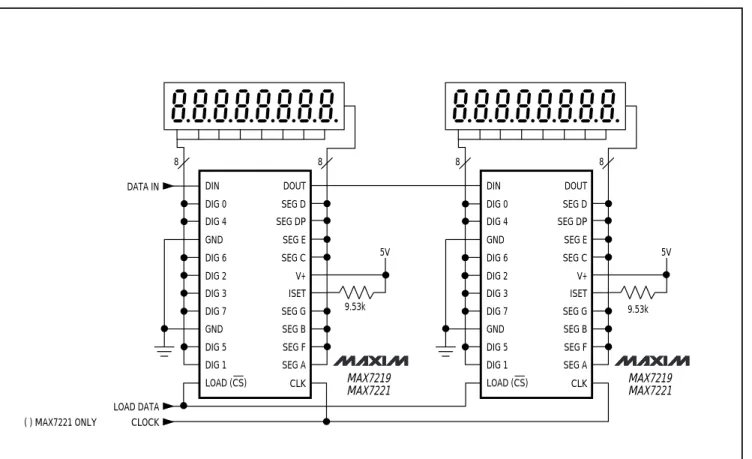
The no-op register is used when cascading MAX7219s or MAX7221s. Connect all devices’ LOAD/CS inputs together and connect DOUT to DIN on adjacent devices. DOUT is a CMOS logic-level output that easily drives DIN of successively cascaded parts. (Refer to the Serial Addressing Modes section for detailed infor-mation on serial input/output timing.) For example, if four MAX7219s are cascaded, then to write to the
fourth chip, sent the desired 16-bit word, followed by three no-op codes (hex XX0X, see Table 2). When LOAD/CS goes high, data is latched in all devices. The first three chips receive no-op commands, and the fourth receives the intended data.
__________Applications Information
Supply Bypassing and Wiring
To minimize power-supply ripple due to the peak digit driver currents, connect a 10µF electrolytic and a 0.1µF ceramic capacitor between V+ and GND as close to the device as possible. The MAX7219/MAX7221 should be placed in close proximity to the LED display, and connections should be kept as short as possible to minimize the effects of wiring inductance and electro-magnetic interference. Also, both GND pins must be connected to ground.
Selecting RSETResistor and
Using External Drivers
The current per segment is approximately 100 times the current in ISET. To select RSET, see Table 11. The
MAX7219/MAX7221’s maximum recommended seg-ment current is 40mA. For segseg-ment current levels above these levels, external digit drivers will be need-ed. In this application, the MAX7219/MAX7221 serve only as controllers for other high-current drivers or tran-sistors. Therefore, to conserve power, use RSET= 47kΩ
when using external current sources as segment dri-vers.
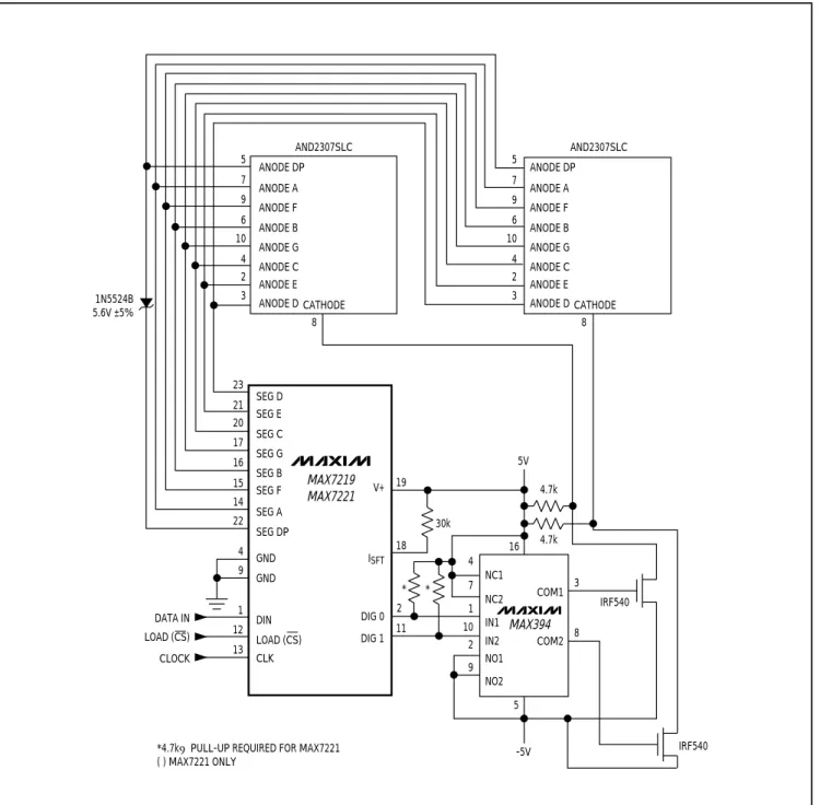
The example in Figure 2 uses the MAX7219/MAX7221’s segment drivers, a MAX394 single-pole double-throw analog switch, and external transistors to drive 2.3” AND2307SLC common-cathode displays. The 5.6V zener diode has been added in series with the decimal point LED because the decimal point LED forward volt-age is typically 4.2V. For all other segments the LED forward voltage is typically 8V. Since external transis-tors are used to sink current (DIG 0 and DIG 1 are used as logic switches), peak segment currents of 45mA are allowed even though only two digits are displayed. In applications where the MAX7219/MAX7221’s digit dri-vers are used to sink current and fewer than four digits are displayed, Table 9 specifies the maximum allow-able segment current. RSET must be selected
accord-ingly (Table 11).
Refer to the Power Dissipation section of the Absolute Maximum Ratings to calculate acceptable limits for ambient temperature, segment current, and the LED forward-voltage drop.
Table 9. Maximum Segment Current for
1-, 2-, or 3-Digit Displays
Table 10. Display-Test Register Format
(Address (Hex) = XF)
10 20 2 MAXIMUM SEGMENT CURRENT (mA) 1 30 3 NUMBER OF DIGITS DISPLAYED X X Normal Operation D6 X X Display Test Mode D4 X X D5 X X D2 X 0 REGISTER DATA D0 X X X D1 X D3 1 X D7 MODENote: The MAX7219/MAX7221 remain in display-test mode (all LEDs on) until the display-test register is reconfigured for normal operation.
Computing Power Dissipation
The upper limit for power dissipation (PD) for the MAX7219/MAX7221 is determined from the following equation:
PD = (V + x 8mA) + (V+ - VLED)(DUTY x ISEGx N)
where:
V+ = supply voltage
DUTY = duty cycle set by intensity register N = number of segments driven (worst case is 8) VLED= LED forward voltage
ISEG= segment current set by RSET
Dissipation Example:
ISEG= 40mA, N = 8, DUTY = 31/32, VLED= 1.8V at 40mA, V+ = 5.25V
PD = 5.25V(8mA) + (5.25V - 1.8V)(31/32 x 40mA x 8) = 1.11W
Thus, for a CERDIP package (θJA = +60°C/W from Table 12), the maximum allowed ambient temperature TAis given by:
TJ(MAX)= TA+ PD x θJA+ 150°C = TA+1.11W x
60°C/W where TA= +83.4°C.
Cascading Drivers
The example in Figure 3 drives 16 digits using a 3-wire µP interface. If the number of digits is not a multiple of 8, set both drivers’ scan limits registers to the same number so one display will not appear brighter than the other. For example, if 12 digits are need, use 6 digits per display with both scan-limit registers set for 6 digits so that both displays have a 1/6 duty cycle per digit. If 11 digits are needed, set both scan-limit registers for 6 digits and leave one digit driver unconnected. If one display for 6 digits and the other for 5 digits, the sec-ond display will appear brighter because its duty cycle per digit will be 1/5 while the first display’s will be 1/6. Refer to the No-Op Register section for additional infor-mation.
MAX7219/MAX7221
Table 11. R
SET
vs. Segment Current and
LED Forward Voltage
Table 12. Package Thermal Resistance
Data
12.2 17.8 1.5 40 11.0 2.5 11.8 30 9.69 15.8 VLED(V) 10.6 29.8 2.0 66.7 20 17.1 14.0 25.9 15.0 28.0 10 3.5 22.6 59.3 3.0 ISEG (mA) 24.5 63.7 55.4 51.2 24 Narrow DIP 24 Wide SO PACKAGE +85°C/W 24 CERDIPMaximum Ambient Temperature (TA) = +85°C Maximum Junction Temperature (TJ) = +150°C
+60°C/W
THERMAL RESISTANCE (θJA)
MAX7219/MAX7221
AND2307SLC ANODE DP ANODE A ANODE F ANODE B ANODE G ANODE C ANODE E ANODE D 5 7 9 6 10 4 2 1N5524B 5.6V ±5% 3 8 8 SEG D SEG E SEG C SEG G SEG B SEG F SEG A SEG DP GND NC1 NC2 IN1*4.7kΩ PULL-UP REQUIRED FOR MAX7221 ( ) MAX7221 ONLY IN2 NO1 NO2 4 3 8 7 1 10 2 5 9 GND DIN LOAD (CS) ISFT V+ 16 COM1 COM2 DIG 1 DIG 0 DATA IN LOAD (CS) CLOCK CLK 4.7k 4.7k -5V 5V 2 11 18 19 * * IRF540 30k IRF540 23 21 20 17 16 15 14 22 4 9 1 12 13 CATHODE ANODE DP ANODE A ANODE F ANODE B ANODE G ANODE C ANODE E ANODE D 5 7 9 6 10 4 2 3 CATHODE AND2307SLC MAX7219 MAX7221 MAX394
MAX7219/MAX7221
( ) MAX7221 ONLY CLOCK LOAD DATA DOUT SEG D SEG DP SEG E GND DIG 4 DIG 0 DIN 5V 8 8 SEG C V+ ISET SEG G DIG 7 9.53k DIG 3 DIG 2 DIG 6 SEG B SEG F SEG A CLK LOAD (CS) DIG 1 DIG 5 GND MAX7219 MAX7221 DOUT SEG D SEG DP SEG E GND DIG 4 DIG 0 DIN 5V 8 8 SEG C V+ ISET SEG G DIG 7 9.53k DIG 3 DIG 2 DIG 6 SEG B SEG F SEG A CLK LOAD (CS) DIG 1 DIG 5 GND MAX7219 MAX7221 DATA IN
MAX7219/MAX7221
_Ordering Information (continued)
___________________Chip Topography
PART MAX7221CNG MAX7221CWG MAX7221C/D 0°C to +70°C 0°C to +70°C 0°C to +70°C
TEMP. RANGE PIN-PACKAGE
24 Narrow Plastic DIP 24 Wide SO Dice* MAX7221ENG MAX7221EWG MAX7221ERG -40°C to +85°C -40°C to +85°C
-40°C to +85°C 24 Narrow Plastic DIP 24 Wide SO
24 Narrow CERDIP *Dice are specified at TA= +25°C.
SEG F SEG A CLK LOAD OR CS DIG 1 DIG 5
GND DIG 7 DIG 3 DIG 2 DIG 6 GND
0.093" (2.36mm) 0.080" (2.03mm) SEG B ISET SEG E SEG DP SEG C SEG G DIG 4 DIG 0 DIN DOUT SEG D TRANSISTOR COUNT: 5267 SUBSTRATE CONNECTED TO GND
MAX7219/MAX7221
________________________________________________________Package Information
MAX7219/MAX7221
___________________________________________Package Information (continued)
SOICW.EPS
Maxim cannot assume responsibility for use of any circuitry other than circuitry entirely embodied in a Maxim product. No circuit patent licenses are implied. Maxim reserves the right to change the circuitry and specifications without notice at any time.